X-Ray Data Booklet
Section 3.2 LOW-ENERGY ELECTRON RANGES IN MATTER
The electron range is a measure of the straight-line penetration distance of electrons in a solid [1]. Electrons with energies in the kilo-electron volt range, traveling in a solid, are scattered inelastically in collisions with the electrons in the material. For low-Z materials, such as organic insulators, scattering from the valence electrons is the major loss mechanism for incident electron energies from 10 eV to 10 keV. The core levels contribute less than 10% to the electron’s energy dissipation for energies between 1 keV and 10 keV [2]. A PDF version of this section is also available.
A. CSDA RANGES
For electron energies below 5 keV, the usual Bethe-Bloch
formalism is inadequate for calculating the electron energy loss in a solid,
and an approach using the dielectric response of the material is used [3].
The complex dielectric function ![]() describes
the response of a medium to a given energy transfer
describes
the response of a medium to a given energy transfer ![]() and
momentum transfer
and
momentum transfer ![]() . The dielectric
function contains contributions from both valence and core electrons. References
4 and 5 describe the steps for calculating
. The dielectric
function contains contributions from both valence and core electrons. References
4 and 5 describe the steps for calculating ![]() for
insulators and metals, respectively. For an electron of energy E, the probability of an energy loss w per unit distance is given
by [2]
for
insulators and metals, respectively. For an electron of energy E, the probability of an energy loss w per unit distance is given
by [2]
![]() (1)
(1)
where![]() and
and
![]() . The quantity
. The quantity ![]() is
also known as the differential inverse mean free path, because by integrating
it over all allowed energy transfers, the inelastic mean free path (IMFP)
is obtained. Furthermore, an integration of
is
also known as the differential inverse mean free path, because by integrating
it over all allowed energy transfers, the inelastic mean free path (IMFP)
is obtained. Furthermore, an integration of ![]() over
all allowed energy transfers gives the energy loss per unit path length, or
stopping power S(E)
The stopping power can then be used to calculate the distance it takes to
slow an electron down to a given energy. This distance is called the continuous
slowing down approximation range, or CSDA range, because the calculation assumes
that the electron slows down continuously from the initial energy E to the final energy, which is usually
taken to be 10 eV [2]. The CSDA range
over
all allowed energy transfers gives the energy loss per unit path length, or
stopping power S(E)
The stopping power can then be used to calculate the distance it takes to
slow an electron down to a given energy. This distance is called the continuous
slowing down approximation range, or CSDA range, because the calculation assumes
that the electron slows down continuously from the initial energy E to the final energy, which is usually
taken to be 10 eV [2]. The CSDA range ![]() is
given by
is
given by
![]() (2)
(2)
The calculations for IMFP and stopping power have been
carried out down to 10 eV for a number of materials, including ![]() [3];
polystyrene [2]; polyethylene [6]; collodion [7]; and silicon, aluminum, nickel,
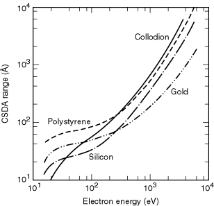
copper, and gold [5]. The CSDA ranges from 15 eV to 6 keV were then calculated
for polystyrene, silicon, and gold by integrating Eq. (2) and are shown in
Fig. 3-3. These curves can be used with confidence down to 100 eV. However,
comparisons of different available calculations with the meager experimental
data below 100 eV indicate that errors as large as 100% may occur at 10 eV.
An example of this is shown in the figure, where experimental range data for
collodion are given. It is clear that the agreement between the collodion
and polystyrene data starts to become reasonable above 100 eV. The differences
below 100 eV could equally well be due to problems with the theory or to the
increased difficulty of the measurement. Stopping-power calculations for polymethyl
methacrylate (PMMA) have been carried out only from 100 eV, so that the CSDA
range as defined above could not be calculated [4]. However, data on effective
electron ranges of photoelectrons in PMMA at several energies can be found
in Ref. 8.
[3];
polystyrene [2]; polyethylene [6]; collodion [7]; and silicon, aluminum, nickel,
copper, and gold [5]. The CSDA ranges from 15 eV to 6 keV were then calculated
for polystyrene, silicon, and gold by integrating Eq. (2) and are shown in
Fig. 3-3. These curves can be used with confidence down to 100 eV. However,
comparisons of different available calculations with the meager experimental
data below 100 eV indicate that errors as large as 100% may occur at 10 eV.
An example of this is shown in the figure, where experimental range data for
collodion are given. It is clear that the agreement between the collodion
and polystyrene data starts to become reasonable above 100 eV. The differences
below 100 eV could equally well be due to problems with the theory or to the
increased difficulty of the measurement. Stopping-power calculations for polymethyl
methacrylate (PMMA) have been carried out only from 100 eV, so that the CSDA
range as defined above could not be calculated [4]. However, data on effective
electron ranges of photoelectrons in PMMA at several energies can be found
in Ref. 8.

Fig. 3-3. Plot of the CSDA range, as a function of energy, for gold and silicon [5] and for polystyrene, (C8H8)n, with a density of 1.05 g/cm3 [2]. The measured electron range in collodion with a density of 1 g/cm3 is also plotted [7].
B. ELECTRON INELASTIC MEAN FREE PATHS
A very important aspect of photoelectron spectroscopy, especially with synchrotron radiation, is the ability to effectively tune the surface sensitivity from a few angstroms or a few tens of angstroms in core-level photoemission measurements to a few hundred angstroms in total-electron-yield surface EXAFS experiments. This variation arises from the fact that the IMFP of the photoemitted electrons is a strong function of the electron kinetic energy, which can be tuned by the appropriate choice of photon energy. The definition of the IMFP [9] is the average distance traveled by an electron between inelastic collisions. Although the exact relationship between the IMFP and kinetic energy depends on the detailed electronic structure of the element or compound of interest, the general features are similar for all elements, starting at large values for kinetic energies below 10–15 eV, dropping to a minimum value of 5–10 Å at kinetic energies between 30 and 100 eV, and then rising monotonically above 100 eV.
Since the surface sensitivity is determined by the depth perpendicular to the surface from which electrons can escape, it is best defined using the mean escape depth (MED), which is related to the IMFP by
D = li cos a , (3)
where D is the MED, li is the IMFP and a is the emission angle of the electrons relative to the surface normal. However, it should be noted that elastic scattering effects within the solid could increase the MED as much as a factor of two at electron emission angles greater than 60°, depending on the angle of incidence of the incoming x-rays and the particular core level being studied [9,10]. Therefore, the standard technique of increasing the surface sensitivity by working at glancing emission angles using Eq. (3) must be qualified to take these effects into account. In addition, both angle-dependent cross sections and photoelectron diffraction effects can result in anisotropic emission from the solid that can also cause errors in the interpretation of the MEDs in solids. Because of these complications, graphs of the IMFPs, rather than the MEDs, versus electron kinetic energy will be presented here to give a measure of the surface sensitivity. The reader is referred to Ref. 9 when more complicated experimental conditions need to be considered.
Using the
formalism developed by Penn that uses optical data to determine the IMFP of
a material [11], Tanuma et al. have calculated the IMFPs for a large number
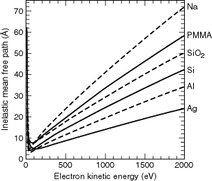
of elements and compounds for kinetic energies up to 2000 eV [12–14]. Figure
3-4 shows IMFP curves for Ag, Al, Na, PMMA, Si, and SiO2.

Fig. 3-4. Inelastic mean free paths for electron kinetic energies up to 2000 eV, for Ag, Al, NA, PMMA, Si, and SiO2.
These materials
are representative of a fairly wide variety of materials for kinetic energies
between 200 and 2000 eV. For example, the IMFPs for Ni, Ta, W, Pt, and Au
all hover around the values given here for Ag; Cr, Fe, and Cu fall between
Al and Ag. Likewise, C falls between Si and SiO2, whereas GaAs
overlies the PMMA curve for much of this energy range. The behavior below
200 eV is more complex, because the IMFPs are strongly dependent on the details
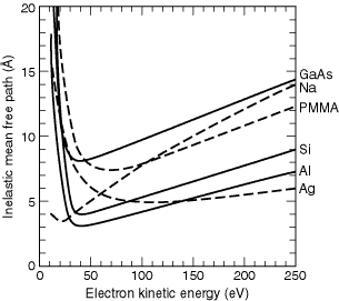
of the electronic structure. Figure 3-5 shows the region below 250 eV for
Al, Ag, GaAs, NA, PMMA, and Si. Silicon dioxide is not shown here because
it overlaps the PMMA curve in this range, whereas GaAs does not. Although
the calculations below 50 eV may not be reliable, owing to limitations in
the theory, the values are plotted at these low energies to show the general
behavior of the IMFPs in this region, as well as the location of the minima
for the different materials.

Fig. 3-5. Detail of the inelastic mean free paths in the kinetic energy range below 250 eV, for Ag, Al, GaAs, NA, PMMA, and Si.
Calculations for additional materials can be found in the literature as follows: (i) elements from C to Bi [12]; (ii) III-V and II-VI compound semiconductors, alkali halides, Si3N4, and several oxides [13]; and (iii) organic compounds [14]. Calculations are being presented here because they provide the most complete and consistent set of values for the IMFPs. References 9 and 10 give the historical background for both the theory and the experimental work in this field and show that it is difficult to generalize much of the experimental data in the literature, owing to the experiment-specific effects described above, as well as uncertainties in sample preparation. Seah and Dench [15] where the first to classify the material dependence of the IMFPs and presented data for kinetic energies up to 10 keV. A good example of the care that is needed in determining IMFPs is given in Ref. 8, which is a study of the Si/SiO2 system. Finally, it should be mentioned that spin-dependent effects on the IMFP have also been observed in ferromagnetic materials [17].
REFERENCES
1. T. E. Everhart and P. H. Hoff, “Determination of Kilovolt Electron Energy Dissipation vs Penetration Distance in Solid Materials,” J. Appl. Phys. 42, 5837 (1971).
2. J. C. Ashley, J. C. Tung, and R. H. Ritchie, “Inelastic Interactions of Electrons with Polystyrene: Calculations of Mean Free Paths, Stopping Powers, and CSDA Ranges,” IEEE Trans. Nucl. Sci. NS-26, 1566 (1978).
3. J. C. Ashley and V. E. Anderson, “Interaction of Low Energy Electrons with Silicon Dioxide,” J. Elect. Spectrosc. 24, 127 (1981).
4. J. C. Ashley, “Inelastic Interactions of Low Energy Electrons with Organic Solids: Simple Formulae for Mean Free Paths and Stopping Powers,” IEEE Trans. Nucl. Sci. NS-27, 1454 (1980).
5. J. C. Ashley, C. J. Tung, R. H. Ritchie, and V. E. Anderson, “Calculations of Mean Free Paths and Stopping Powers of Low Energy Electrons (< 10 keV) in Solids Using a Statistical Model,” IEEE Trans. Nucl. Sci. NS-23, 1833 (1976).
6. J. C. Ashley, “Energy Losses and Elastic Mean Free Path of Low Energy Electrons in Polyethylene,” Radiat. Res. 90, 433 (1982).
7. A. Cole, “Absorption of 20 eV to 50 keV Electron Beams in Air and Plastic,” Radiat. Res. 38, 7 (1969).
8. R. Feder, E. Spiller, and J. Topalian, “X-Ray Lithography,” Polymer Eng. Sci. 17, 385 (1977).
9. C. J. Powell, A. Jablonski, I. S. Tilinin, S. Tanuma, and D. R. Penn, “Surface Sensitivity of Auger-Electron Spectroscopy and X-Ray Photoelectron Spectroscopy,” J. Elect. Spectrosc. 98–99, 1 (1999).
10. A. Jablonski and C. J. Powell, “Relationships between Electron Inelastic Mean Free Paths, Effective Attenuation Lengths, and Mean Escape Depths,” J. Elect. Spectrosc. 100, 137 (1999).
11. D. R. Penn, “Electron Mean-Free-Path Calculations Using a Model Dielectric Function,” Phys. Rev. B 35, 482 (1987).
12. S. Tanuma, C. J. Powell, and D. R. Penn, “Calculations of Electron Inelastic Mean Free Paths. II. Data for 27 Elements over the 50–2000 eV Range,” Surf. Interface Anal. 17. 911 (1991).
13. S. Tanuma, C. J. Powell, and D. R. Penn, “Calculations of Electron Inelastic Mean Free Paths. III. Data for 15 Inorganic Compounds over the 50–2000 eV Range.” Surf. Interface Anal. 17, 927 (1991).
14. S. Tanuma, D. J. Powell, and D. R. Penn, “Calculations of Electron Inelastic Mean Free Paths. V. Data for 14 Organic Compounds over the 50–2000 eV Range,” Surf. Interface Anal. 21, 165 (1991).
15. M. P. Seah and W. A. Dench, “Quantitative Electron Spectroscopy of Surfaces: A Standard Data Base for Electron Inelastic Mean Free Paths in Solids,” Surf. Interface Anal. 1, 2 (1979).
16. F. J. Himpsel, F. R. McFeely, A. Taleb-Ibrahimi, and J. A. Yarmoff, “Microscopic Structure of the SiO2/Si Interface,” Phys. Rev. B 38, 6084 (1988).
17. H. Hopster, “Spin Dependent Mean-Free Path of Low-Energy Electrons in Ferromagnetic Materials,” J. Elect. Spectrosc. 98–99, 17 (1999).